|
Introducing the nanoCam™
An Ultra-Miniature Multi Lens Array 3D Camera
Ultra-Miniature cameras are frequently used today in many areas of consumer applications. The most well known to the public are mobile phone cameras. Other areas are, medical imaging of the interior body, surveillance and homeland security and special effects cinematography.
Today’s digital cameras consist of:
• Large conventional external lenses to focus the image
• Light harvesting elements to increase efficiency or perform ‘plenoptic’ functions
• A light sensitive CMOS layer which collects the image
• Cameras continue to get smaller but decreasing size and sharpness of the single lens
limits the size to which they can be shrunk and usefully function.
• NanoLight’s nanoCam™ performs all of these functions in a totally flat package.
These cameras continue to get smaller and the cmos chip includes an increasing
number of pixels. Decreasing size and sharpness with the single lens employed
in conventional cameras currently limits the size of a useful camera.
This becomes irrelevant with nanoCam™.
How the nanoCam™ Works
The nanoCam™ concept sidesteps the old external lens, allowing the camera to overcome physical-optical limitations to become truly nanosized. This revolutionary technology allows a high definition mega-pixel camera to be flattened to about the width of a human hair. The idea behind the nanoCamera™ is to replace the external lens and collapse the entire apparatus into a sandwich including induction or battery powered circuitry, pixel layer and nanoLens™ array layer. Each nanoLens™ rests over an individual light harvesting element consisting of a number of pixels, the number depending on the limit of the lens. Each of these nano-assemblies become literally nanosized cameras receiving fuzzy images. Through computerized interpolation transformation of each of the images from the nano-assemblies it is possible to present the observer with a single high resolution image. Related methods are employed in large astronomical telescopes when analyzing fuzzy information. In fact it is possible with such a composite to fabricate a sensing field with a larger combined aperture than conventional lenses or mirrors. As each element receives slightly different spatial (angular) information from the observed object it also becomes possible to render 3D imaging and depth information.
The principles behind nanoCam™ have been recently verified by research at major universities. New research also has demonstrated the transmission of light through smaller than wavelength apertures, opening up the prospect of smaller scaling than previously thought possible.
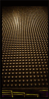
nanoCam™ Construction
 |
+ |
 |
+ |
 |
= |
 |
| nanolens™ array layer |
|
pixel layer |
|
circuitry layer |
|
Section of sandwiched nanoCam™ 1/500mm wide |
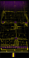
Multi-lens Image Enhancement
 |
> |
 |
| single element nanolens™ will create a fuzzy image |
|
|
 |
> |
 |
| multi-element nanolens™ array will create an enhanced image |
|
|
nanoCam™ Applications
Higher resolution is only the beginning of applications opened by the use of multiple camera elements at the nano level in particular. Nano sized optical apertures can uniquely be made to suppress certain light frequencies and can be made sensitive to a broad or selective range of radiation. The nanoCam™ technology is not limited to acquiring images of visible light only. This technology instead opens up entirely new possibilities of gathering wide ranging optical data that can deliver beyond what is conventionally obtainable. Examples of such information includes heat radiation (IR), UV, and chemical emission spectra all in the same instrument. The advantages of overlaying such extra sensory information on conventional visible images is to create a chemical map over the image adding little additional size. The nanoCamera™ can indeed become so small that it is virtually invisible and by integrating transmitting devices it will be possible to have a featherweight reporting or surveillance device many times smaller and flatter than anything now achievable. Its light weight will be well suited to micro UAV reconnaissance aircraft, and as mentioned be able to analyze chemical spectra.
Such a device will be ideal to monitor and transmit images from the interior body areas inaccessible even to micro medical devices and will be usable in capillary sized areas and neuro-medical imaging. The tiny flat nanoCam™ device made primarily of silicon may be implanted in contact lenses and in the eye itself,even wirelessly connecting to occipital neural implants.Treating blindness or bionic enhancement of ordinary vision will become a reality.
Additional Advantages of the Ultra Thin nanoCam™
The wafer thin composite can be made to assume many forms, for instance, it can be wrapped or fabricated in a spherical shape to produce a true 360 degree image, or separated into widely spaced, dust sized elements which wirelessly communicate with one another, or with a central processor, like GPS satellites.
nanoCam™ is not merely a ‘camera’. It can be a nanochip in optical computing for interface routing or a mega-channel optical signal processor and when CMOS sensors are augmented by LEDs a transmitting projector.
Basic to nanoCam™'s nature is an extremely small focal length and nearly infinite depth of field which may not require auto focus mechanisms. On the other hand a large flat spread could easily obtain selective focus. As pointed out, 3D imaging can also be obtained through software with these flexible multiple elements.
Through material fabrication techniques, tailoring the optical properties even optical zooming is possible, however multiple single focal length elements offer simpler fabrication and distinct advantages such as a camera system on a chip or a credit card, to a very large flat space telescope, rolled or folded for transport. It is possible for a flat 1 meter telescope to achieve tera-pixel resolution. With spaced arrays interstellar planetary data can become a reality.
Market
The interest in nano cameras will increase rapidly in the next few years as more and more consumer products are being launched and the military applications are considered. We estimate the phone camera market alone to be around $100 Billion. The consumer camera market is $25 Billion. The market for the nano-camera is estimated at around $100 Million.
For further information or inquiries please contact :
info@nanolighttechnologies.com
|